The detail description of MOSFET parameters in the datasheet
There are many related parameters in the MOSFET data manual. Take the MOSFET 7N60 as an example. Let's take a look at the parameters that are generally included in the MOSFET data manual.
The limit parameter is also called the absolute maximum rated parameter. During use, the MOSFET must not exceed these limit parameters in the following figure, otherwise the MOSFET may be damaged.
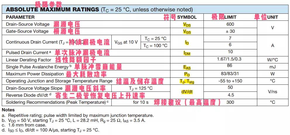
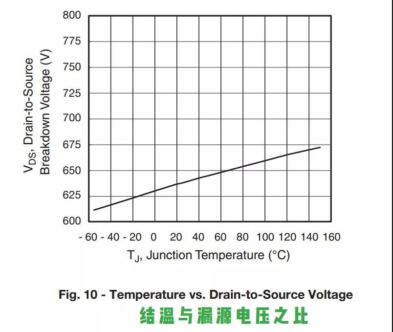
VDS represents the maximum voltage value that can be applied between the drain and the source.
VGS represents the maximum voltage value that can be applied between the gate and the source.
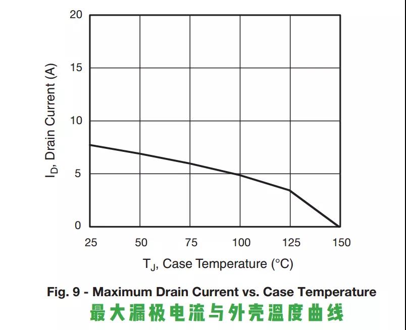
ID represents the continuous current value that the drain can withstand. If the current flowing exceeds this value, it will cause a risk of breakdown.
IDM indicates the current intensity of a single pulse between the drain and the source. If this value is exceeded, it will cause a risk of breakdown.
EAS stands for single-pulse avalanche breakdown energy. If the voltage overshoot (usually due to leakage current and stray inductance) does not exceed the breakdown voltage, the device will not undergo avalanche breakdown, so there is no need to dissipate the avalanche breakdown ability. EAS calibrates the level at which the device can safely absorb reverse avalanche breakdown energy.
PD stands for the maximum power dissipation, which refers to the maximum drain source power dissipation allowed when the performance of the MOS does not deteriorate. When using it, pay attention to the actual power consumption of the MOS should be less than this parameter and leave a certain margin, this parameter will generally As the junction temperature rises, it is reduced. (This parameter is not reliable)
TJ, Tstg, these two parameters calibrate the junction temperature range allowed by the device's working and storage environment. Avoid exceeding this temperature and leave a certain margin. If you ensure that the device works within this temperature range, it will greatly extend its life span.
dV / dt reflects the ability of the device to withstand the rate of voltage change, the greater the better. For the system, too high dv / dt will inevitably bring high voltage spikes and poor EMI characteristics, but the rate of change can be corrected by the system circuit.

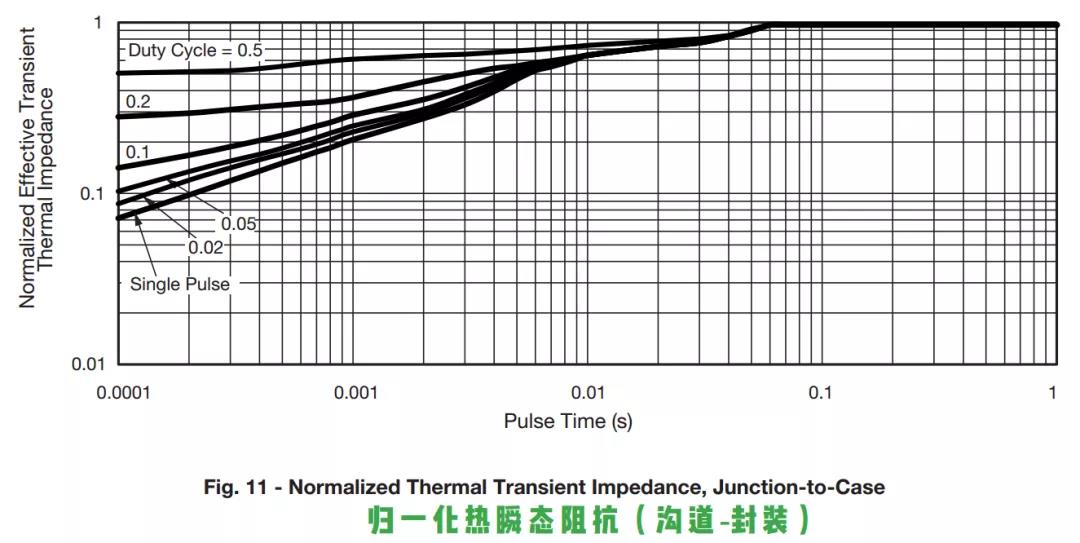
Thermal resistance indicates the difficulty of thermal conduction. Thermal resistance is divided into the thermal resistance between the channel and the environment and the thermal resistance between the channel and the package. The smaller the thermal resistance, the better the heat dissipation performance.

△ VDS / TJ represents the temperature coefficient of the drain-source breakdown voltage, the positive temperature coefficient, the smaller the value, the better the stability.
VGS (th) represents the turn-on voltage (threshold voltage) of MOS. For NMOS, when the applied gate control voltage VGS exceeds VGS (th), NMOS will turn on.
IGSS represents the gate drive leakage current. The smaller the better, the system efficiency will be affected to a lesser extent.
IDSS represents the drain-source leakage current. The drain-source leakage current when the gate voltage VGS = 0 and VDS is a certain value is generally in the microampere level.
RDS (ON) represents the on-resistance of MOS. Generally, the smaller the on-resistance, the better. It determines the on-loss of MOS. The larger the on-resistance, the greater the loss and the higher the temperature rise of MOS. In, the conduction loss will account for a larger proportion of the total loss of the MOS.
gfs represents the forward transconductance, reflecting the ability of the gate voltage to control the drain-source current. Too small gfs will cause the MOSFET to turn off at a reduced speed, the ability to turn off will be weakened, too large will lead to too fast turn off, poor EMI characteristics, and With the turn-off, the drain source will generate a larger turn-off voltage spike.
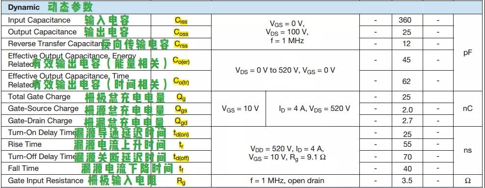
Ciss represents the input capacitance, Ciss = Cgs + Cgd, this parameter will affect the MOS switching time, the larger the value, the slower the turn-on and turn-off time under the same driving capacity, the greater the switching loss.
Coss means output capacitance, Coss = Cds + Cgd; Crss means reverse transmission capacitance, Crss = Cgd (Miller capacitance). These two parameters have a slight impact on the MOSFET turn-off time. Among them, Cgd will affect the amount of energy transferred to the gate of the MOSFET when the drain has an abnormally high voltage, which will have a certain impact on the lightning test item.
The parameters Qg, Qgs, Qgd, td (on), tr, td (off), and tf are all related to time. The faster switching speed corresponds to the advantages of smaller switching losses, higher efficiency, and lower temperature rise. The corresponding disadvantages are poor EMI characteristics and excessively high MOSFET turn-off spikes.

If the IS and ISM parameters are too small, there is a risk of current breakdown.
If VSD and trr are too large, it will cause excessive system loss and excessive temperature rise in the bridge or LCC system.
Qrr This parameter is proportional to the charging time, generally the smaller the better.
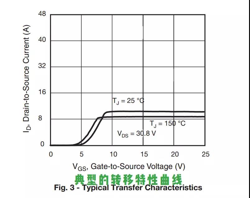
The output characteristic curve is used to describe the relationship between the current and voltage of the MOSFET. The characteristic curve will be affected by the junction temperature. The general data manual will list the characteristic curves at two temperatures.
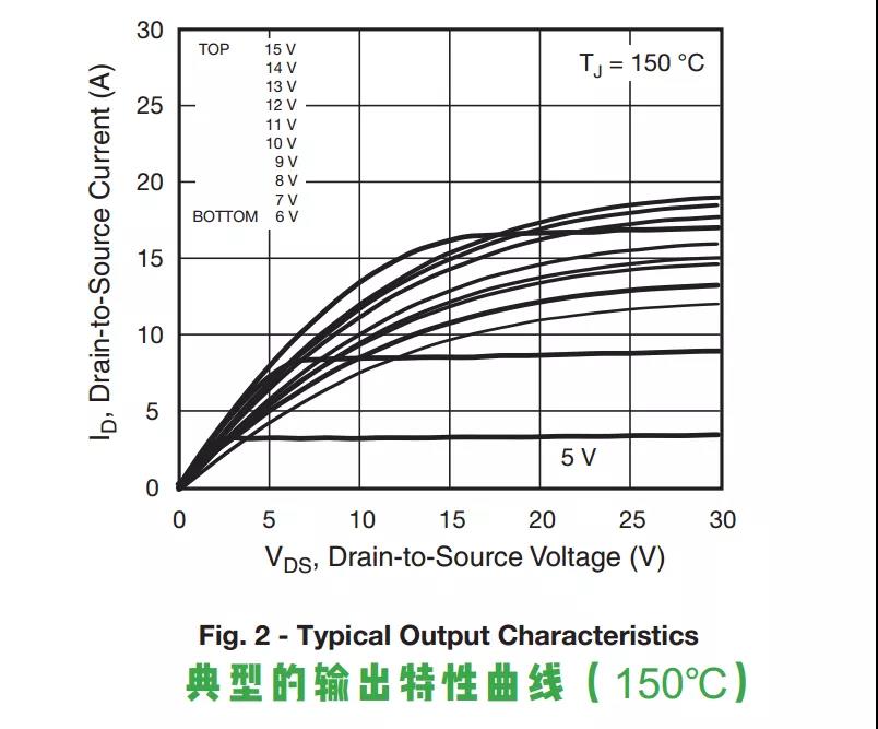
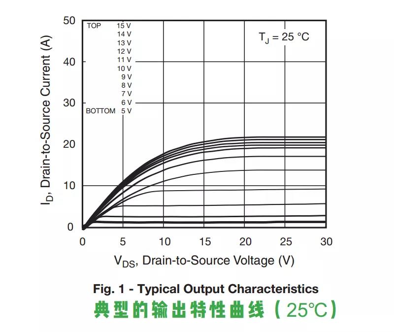
According to the output characteristic curve of the MOSFET, take one of the Uds and then use it as a method of the graph to obtain the corresponding transfer characteristic curve. It can be seen from the transfer characteristic curve that when Uds is a certain value, the relationship between Id and Ugs.
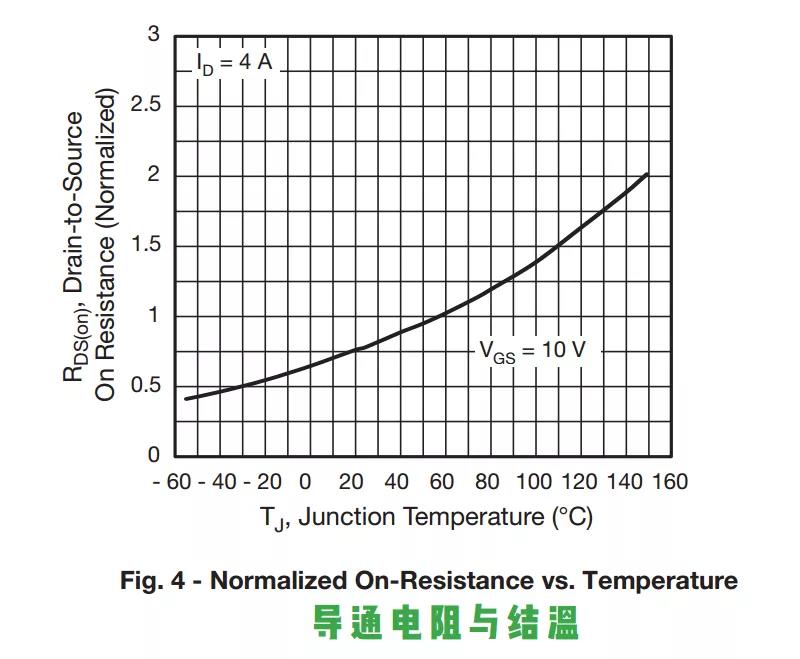
The on-resistance and junction temperature of MOS change with a positive temperature coefficient, that is, the higher the junction temperature, the greater the on-resistance. The MOS data sheet generally draws the curve of the on-resistance with temperature when VGS = 10V.
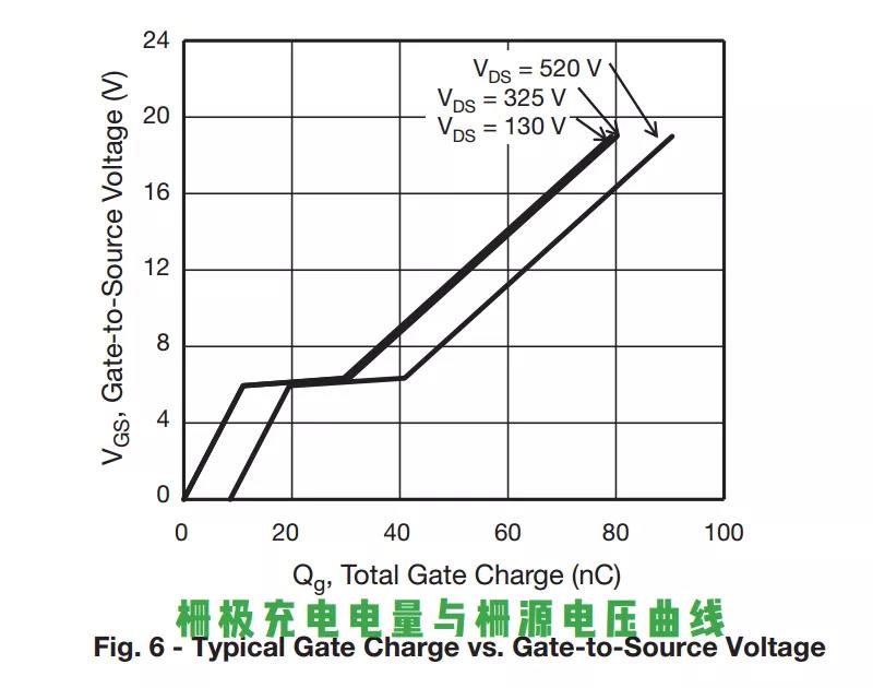
The smaller the capacitance value, the smaller the total gate charge QG, and the faster the switching speed, the smaller the switching loss. Applications such as switching power supply DC / DC converters require a smaller QG value.
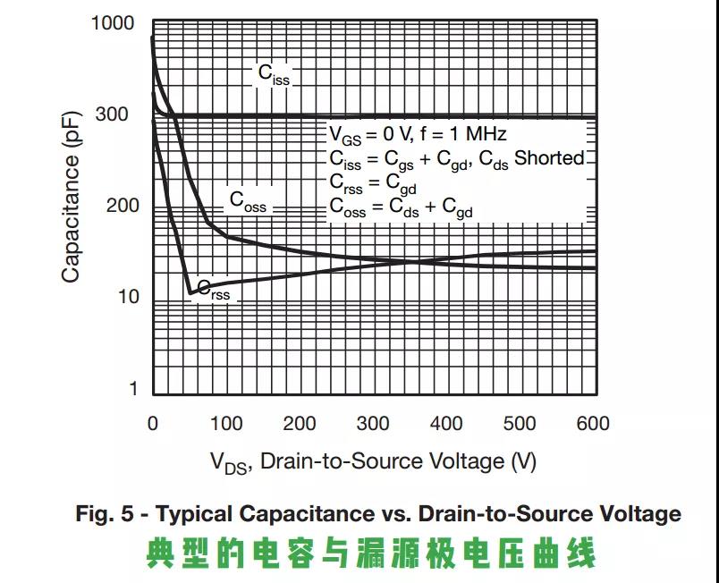
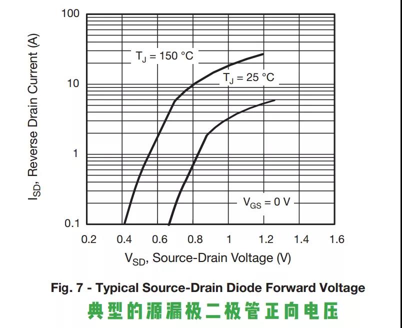
The MOSFET generally has a parasitic diode. The parasitic diode has a protective effect on the MOSFET . Its characteristics are the same as ordinary diodes, and it also has the characteristics of forward conduction.
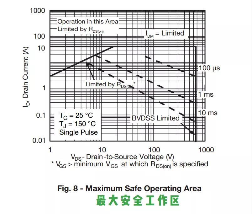
The maximum safe working area is a two-dimensional area formed by a series of (voltage, current) coordinate points. The voltage and current of the MOSFET during operation cannot exceed this area. If it exceeds this area, there is danger.
It can be seen that there are actually many relevant parameters of the MOSFET. In fact, in general applications, we mainly consider the drain-source breakdown voltage VDS, continuous drain current ID, on-resistance RDS (ON), maximum power dissipation PD Parameters such as turn-on voltage VGS (th), switching time, operating temperature range, etc. are sufficient.